Several people wrote a reply to RFI W911NF-20-RFI-QCF, which was submitted October 6, 2020. The final files appear below followed by an approximate WordPress rendition of the main document.
The organizers ask for an optional PowerPoint slide
and as a PowerPoint (.ppt) file
The document has been pasted into HTML format. HTML format is not the same as pdf format.
Quantum Access
Response to W911NF-20-RFI-QCF
Erik DeBenedictis, Zettaflops LLC (POC)
1415 Canyon Rim Dr., NE
Albuquerque, NM 87112
(505) 440-2176
erikdebenedictis@zettaflops.org
Michael Hamilton, Auburn University
200 Broun Hall
Auburn University, AL 36849
o: (334) 844-1879 f: (334) 844-1888
mchamilton@auburn.edu
Oleg Mukhanov, SeeQC
175 Clearbrook Road
Elmsford, NY 10523
(914) 393-5055
omukhanov@seeqc.com
October 6, 2020
Group support statements:
Bryan Tyrrell: “Lincoln Laboratory has active R&D efforts in relevant technologies and has indicated a willingness to work collaboratively to support potential quantum access efforts in a manner consistent with its role as a Federally Funded Research and Development Center.”
John D. Cressler, Georgia Tech: “As a university researcher active in this field, and a frequent user of multi-project wafer (MPW) electronic and photonic fabrication, having such a venue in the quantum domain would dramatically accelerate research and development, as well as facilitate student training, and thus I find the vision both compelling and exciting. I would be happy to collaborate with the team as it moves forward.”
Eby Friedman, Rochester: “As a likely end-user at the academic level and deeply involved in quantum-based circuits and systems, a source of fabrication of superconductive qubits and related cryogenic quantum circuits would be seminally important in demonstrating and validating our novel circuitry.”
Shawn Fetterolf/Robert Freeman, Synopsys: “Synopsys is actively developing TCAD and EDA tools for Superconducting Electronics under the IARPA SuperTools program. Synopsys expects that these tools and their derivatives will be valuable for developing Superconductor-based qubits and interfaces for quantum computing and to that end supports the Quantum Access initiative for widening access to quantum hardware prototyping facilities by industry and universities.”
Gordon Harling, CMC: “CMC Microsystems provides cost-shared infrastructure for CAD tools and MPW fabrication services in microelectronics, photonics, and microelectromechanical systems (MEMS). We are pleased to be a partner in this quantum initiative and to contribute to the network.”
Britton Plourde, Syracuse University: “A quantum access program would be beneficial to academic research groups in quantum information science. This would be particularly useful for new researchers without existing fabrication capabilities of their own. In addition, established groups may also benefit through access to advanced fabrication that is not possible with their own facilities. Such a program could potentially be utilized in future advanced quantum engineering courses at the graduate or possibly even undergraduate levels for designing qubits and having them fabricated.”
Celia Merzbacher, QED-C: “Members of QED-C identified the need and voiced support for small-volume fabrication capabilities to facilitate research and development of chip-level components for qubit control at a recent workshop (September 2020) on electronics and RF/microwave components for control of quantum systems. QED-C supports the exploration and realization of a program to fill this need and that would broadly benefit the QIS supply chain.”
Quantum Access
Executive Summary
Quantum information is an important new direction for the current electronics industry. To successfully exploit quantum information will require education and innovation in both hardware and software as well as the development of commercial infrastructure for design and manufacture of quantum components.
This RFI response is from three co-authors that are part of an IEEE interest group on the topic, one organizing the group (DeBenedictis), another that runs a fab (Mukhanov), and the third from a university (Hamilton) that accesses fab services in support of education and research.
It is crucially important for fabs and end users to share needs, capabilities, and business models. Small-volume users are often the most innovative, yet their nimbleness is a result of improving one aspect of a system at a time without the need to build an entire system from scratch. However, fabs are most profitable with large volumes, which goes along with business arrangements that are complex, challenging, and often prohibitively expensive for small users.
The goal of this RFI response is to present a common ground approach to the complex process in the previous paragraph, similar in many ways to the approach put forth to justify DARPA MOS Implementation Service (MOSIS) in the early 1980s and more recently the Trusted Access Program Office (TAPO). Since then, these services have acted as an intermediary between small users and multiple entities that perform the fabrication, aggregating small CMOS projects into multi-project wafers/runs, fabbing them, and ultimately returning packaged chips to users.
Just as MOSIS launched with one CMOS line, the authors’ view is that superconductor qubits (transmons) and associated cryogenics and support electronics are at a similar stage of maturity today and ready for a similar service that we tentatively call Quantum Access here. Spin qubits, ion traps and other future qubit technologies will fit within the framework later.
A Brief History of Innovation in Integrated Electronics
Integrated electronics started out as integrated passive components and bipolar junction transistors, with the switchover to MOSFETs leading to substantial scale up of the resulting systems and the emergence of infrastructure for design, prototyping, and manufacturing.
The current interest in integrated quantum systems clearly envisions engaging and enhancing the current semiconductor ecosystem to attempt to achieve similar scale-up. Details of qubit fabrication should be covered by other responses to this RFI, so this RFI response will concentrate on delivering a service in the most useful way.
Today’s superconducting (e. g. transmon) qubits are at a similar stage of maturity to MOSFETs circa 1980. In both cases, companies created integrated systems using proprietary design tools and in-house fabs. Irrespective the unique nature of each manufacturer’s approach, DARPA launched the MOSIS effort to create process-independent design rules that allowed students and innovative researchers to share space on affordable and convenient multi-project wafers (MPW).
In both cases, specialization is essential for a technology that advances through scale up. While the best transistors and qubits are unique in both their materials and design, the resulting systems are not made entirely of one device type. They include electrical amplifiers, microwave components, thermal components, and a diverse set of components for other functions. An improved amplifier can usually be tested with the last generation of qubits or DRAM bits, etc., just as the next generation of qubits can be tested by the existing generation of amplifiers and microwave infrastructure. Thus, as systems become more complex, a student or innovator will need to focus on one aspect of a complex system, leading to distinct roles for efficient prototyping on the one hand and efficient systems integration on the other.
Just as the earliest MOSIS supported only one CMOS variant, this document applies to superconducting qubits today, but the concept will expand to encompass spin qubits, ion traps, and other approaches over time.
“Quantum Access”
The vision is that Quantum Access would include a non-profit operator that would aggregate small user designs into the quantum equivalent of a multi-project wafer/run, while handling funding and business relationships to and from both sides. Quantum Access should also include a less formal association of users and suppliers that would find best practices and set informal standards for efficient use of the fabs as well as testing, demonstration, and publishing of results.
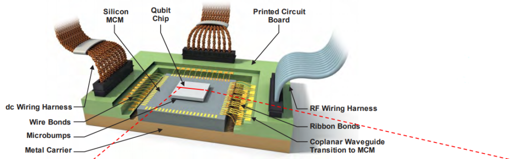
Fig. 1 shows a module that can clarify Quantum Access. The module in fig. 1 includes both qubits and control electronics, intended to be used in a cryogenic environment. While creating the module the first time was an original research project beyond the proposed capability of Quantum Access, duplicating the module is less risky. As described above, the real goal is not exact duplication, but, for example, retrofitting an innovative qubit design into an otherwise proven test platform.
Thus, even though Quantum Access may not create systems that are state-of-the-art in every respect at once, it would enable students to become proficient with the technology while in school and allow innovators to advance the state-of-the-art in many areas in parallel.
In the authors’ vision, Quantum Access would:
- contract with fab houses to fabricate qubits (the small, highlighted, rectangle in fig. 1) and/or control electronics (the larger base), optionally packaging the components, sending the bare die or packaged modules to the user.
- at the business level, the operator would contract with fabs, design tool suppliers, and companies that can perform the assembly activities, aggregating funds from small users to create fabrication runs that are compatible with standard industrial jobs.
- organize, but not create, and arrange distribution of educational materials, process design kits (PDKs), and generic intellectual property (IP) that enables users to get up to speed quickly.
Quantum Access Status and Next Steps
The status of the Quantum Access concept is that IEEE has an internationally scoped interest group in this area (https://fab.quantum.ieee.org), which has participation from the major quantum-relevant fabs, universities, and users in the USA. IEEE can serve a coordinating function in the long term. There is also member overlap and coordination between the IEEE interest group and the Quantum Economic Development Consortium (QED-C).
As first steps, superconducting qubits, cryogenics, and classical electronics including passives, cryogenic CMOS, and Josephson junctions are at a maturity level suitable for the Quantum Access concept. With agreement between parties and a small amount of funding it would be possible to follow and document the processes used by existing quantum projects and have them reviewed by the community as the first process for a Quantum Access operator. This could be a function for the IEEE interest group.
It will be crucially important to have informal standards and basic IP for efficient use of Quantum Access. US Government programs such as SuperTools and their performers are part of the IEEE interest group and these tools should be a part of a program as soon as they are ready. Likewise, some “open source” designs for qubits and support functions are believed to be ready and would be helpful. In fact, there has been discussion in the interest group that could be explained in a meeting about how Quantum Access could work within a hierarchy of IP sensitivity levels, ranging from “open source” to government-level sensitivity.
Qubits
The authors believe the following fab capabilities could enable a lot of education and innovation and could form a first step for Quantum Access. The rest of this section addresses technical details such as ground plane, Josephson junctions, integration, and metrology.
Ground Plane and Wiring: The facility for fabricating superconducting qubits should have the capability of depositing and patterning high quality, low loss niobium (Nb) films on high resistivity silicon to form the ground plane, wiring layer, shunt capacitors, microwave cavities, etc. that support control and readout of the qubits. As a benchmark of film quality, we should expect microwave resonators patterned on such films and cooled to T~10mK to have quality factors around 106. The processes/equipment needed to meet these requirements are as follows:
- Buffered Oxide Etch: A buffered oxide etch to remove oxide from silicon wafers to produce the best wafers.
- Sputter Deposition System: A sputter deposition system capable of depositing good quality Nb films. The system should be cryo-pumped with a base pressure p<1×10⁻⁷ mBarr. It is important that the system is not used to deposit any metals which could contaminate the Nb film (i.e. magnetic materials).
- Optical Lithography System: An optical lithography system for patterning the ground plane layer. It should have a resolution <1µm.
- Reactive Ion Etch System: An RIE with SF6 process gas that can be used to etch the niobium film.
Josephson Junctions: All superconducting qubits in use today are based on one or more Josephson Junctions (JJs) employed as nonlinear inductors. Thus, in addition the above, Quantum Access would require a process to fabricate high quality JJs. The process should have the capability to produce JJs with areas around 100 nm × 100 nm and critical current density JC ~ 1 µA/µm2 (or total critical current IC ~ 10 nA). In terms of reproducibility, the normal state resistance of the tunnel barrier should be controllable to within 10% for flux tuneable qubits, and to within 1% for fixed frequency qubits. To produce quality JJs with such small areas easily and reliably requires:
- Electron Beam Lithography (EBL) System: An EBL with resolution less <100nm. It should have accelerating voltage 100kV and write speed that is fast enough that we can pattern a whole wafer in a practical time. Exemplary tool – JEOL 8100FS EBL
- Electron Beam Thermal Evaporator:A thermal evaporation system dedicated to producing aluminium Josephson junctions. The system should have a base pressure <3×10⁻⁸ mbarr and substrate holder that can rotate around 2 axes. Exemplary tool – Plassys MEB550s
Integration and Metrology: To ease integration of multiple qubits, packaging, and screening of fabricated qubit samples, these capabilities are suggested:
- Vertical Integration: The ability to fabricate superconducting crossovers (air bridges) and thru silicon vias (TSVs) is needed to enable multi-qubit circuits with more complicated wiring patterns. In addition, a foundry should have the ability to join a qubit chip to another chip through superconducting bumps in a multi-chip module (MCM), with a controlled and uniform gap between the two chips.
- Testing and Auxiliary: An auto wafer probe station is suggested to quickly screen Josephson Junctions at room temperature to check that the normal state resistance is within spec. This will prevent costly and time-consuming low temperature tests being performed on bad qubits. The cryogenic wafer probe station, like that developed by BlueFors for Intel is desirable. The foundry should have a wafer saw for dicing individual chips from the larger wafer for testing at millikelvin temperatures.
Educational and Small Research Users
Based on experience from our IEEE working group, the main goal of university researchers and educators is to properly prepare undergraduate and graduate students and researchers so that they will be part of a ready and contributing workforce. The complexities and challenges of quantum systems make significant hands-on experience an imperative. While many universities have micro/nano fabrication tools and characterization capabilities for semiconductors now, the challenges mentioned in the RFI are barriers to faculty, such as in computer engineering/architecture. Multiple members of our working group would engage with and pursue using a QC research foundry facility.
Informed by the general ideas above, Hamilton’s group at Auburn can give more specific views from first had experience. Hamilton’s group currently focuses on packaging/interfacing/ integration technology, using unpackaged, lightly characterized chips with not-necessarily-complete designs. This group may expand over time to packaged, highly-characterized chips with essentially “turn-key” qubits and associated control/read-out components.
We focus on packaging and integration technologies for superconducting qubit technologies and would like to explore the impact of these technologies on stable, uniform superconducting qubit technologies. We also have efforts in cryogenic materials characterization and new quantum materials, as well as quantum state transduction, all of which we would like to integrate with high performance superconducting qubits to better engineer these systems. Qubit design flexibility in the form of new device designs/geometries would be desired. Incorporation of novel materials could be an interesting approach in the future, especially if it could be in the form of post-processing or heterogenous integration of chips or wafers in our research labs.
Based on pre-quantum experience, process stability is a concern. Successful Si-based technologies are locked-down and must be stable and unchanging to allow wider adoption. There could be two (or more) tracks for quantum fabrication runs, or multiple foundries, where one is the stable track with a planned technology advancement path, while the other is more of a research track that allows new fabrication methods/materials to be explored.
As an academic research group, we do not necessarily have a breakpoint for $/chip. Academic pricing on par with other technology access entities (i.e., MOSIS, MEMSCAP, X-FAB, etc.) would be workable.
- We use MOSIS/TAPO without help and we hope the same will apply to quantum technologies.
- We currently do microwave/RF engineering, modeling, etc., yet information in the PDK about known good designs would be useful.
- We have had challenges at times with legal/paperwork aspects of interacting with external fabrication entities.